23. Embrittlement of Cu Micro-Structures
Copper metallization layers in semiconductor devices have distinct advantages over those made of aluminum due to their higher electrical and thermal conductivity. In order to improve the mechanical strength of these layers, additives are usually introduced during the electrodeposition process to reduce the grain size in the microstructure in the spirit of the Hall-Petch effect [2], [3]. However, some of these additives actually lead to embrittlement of the microstructures at elevated temperatures [4]. Ab initio DFT calculations help to unambiguously identify the type of impurities causing this detrimental behavior as well as the mechanisms leading to fracture [4].
Keywords: semiconductors device, metallization layer, copper, microstructures, embrittlement, grain boundaries, impurities, segregation
23.1. Background
In the race for still smaller structures of semiconductor devices, copper metallization layers have a significant advantage over those made of aluminum, since their much higher electrical and thermal conductivity allows for smaller metal components and less energy consumption. However, long-term stability of the devices requires also a high mechanical performance of the metal contacts. Fortunately, the mechanical properties of such microstructures can be controlled and considerable improved by reducing the grain size, which is well known as the Hall-Petch effect [2], [3]. Indeed, for electrodeposited Cu thin films it has been demonstrated that additives can cause a reduction of the grain size. However, as revealed by electron backscatter diffraction in a scanning electron microscopy (EBSD/SEM), these additives at the same time caused embrittlement of the microstructures at elevated temperatures [4]. The present application note describes how ab initio calculations based on density functional theory (DFT) can be employed to obtain a deeper understanding of the origin of this failure [4].
23.2. Experimental Findings
In the experiments reported in [4], Cu thin films were synthesized by electrodeposition using two different additive systems in the electrolyte with the aim to modify the grain size (sample type A and B). EBSD/SEM images of these films are displayed in Figure 23.2.1. Samples of types A and B possess median grain sizes of about 2.7 ± 0.6 µm and 10.1 ± 2.6 µm, respectively. As also shown in Figure 23.2.1, the grain size of sample type A could be increased by additional annealing at 1073 K.

Figure 23.2.1 EBSD/SEM images of the surface and cross-section of the tensile-samples. (a, b, c) Sample type A, (d) sample type A annealed at 1073 K for 5 h, (e, f, g) sample type B and (h) color code of the inverse pole figure corresponding to the grain orientations. Note that the distortion in (g) is caused by a curved surface.
Mechanical testing revealed distinct differences between the two sample types as is obvious from Figure 23.2.2. While at room temperature sample type A exhibited considerable higher yield strength and ultimate tensile strength as compared to sample type B as expected from the Hall-Petch effect, this supremacy is lost at elevated temperatures, where sample type A showed a drastic reduction in yield strength, ultimate tensile strength, and elongation to fracture. In contrast, sample type B showed only a moderate decrease of these values.
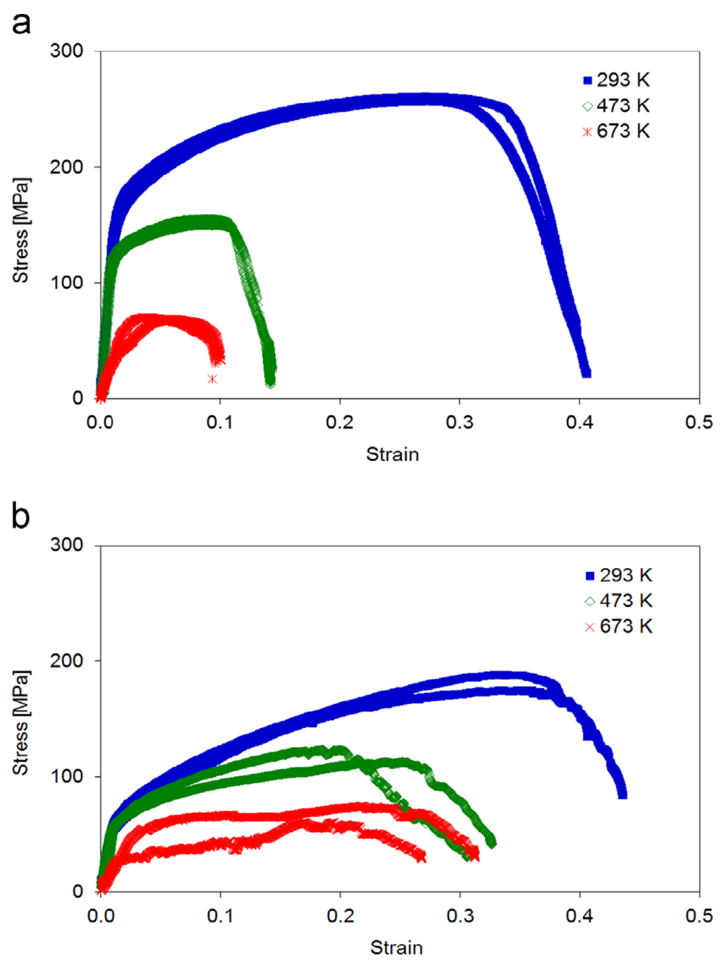
Figure 23.2.2 Stress–strain curves of sample types A and B at 293 K, 473 K and 673 K. Note that at 473 K the yield strength, ultimate tensile strength and elongation to fracture are drastically smaller for the (a) fine-grained sample type A compared to (b) samples of type B with their bamboo-like microstructure. The ultimate tensile strength shows a significant decrease with increasing temperature. Both sample types A and B show a significantly smaller slope during loading at 673 K (apparent Young’s modulus) caused by plastic deformation (settlement) of the sample head.
SEM images of sample type B taken at 293 K, 473 K, and 673 K clearly showed ductile behavior with intragranular fracture accompanied by the formation of glide steps at all temperatures. In contrast, sample type A showed strong plastic deformation with several grains involved at 293 K, whereas at higher temperatures the cracking occurred preferentially along the grain boundaries indicative of grain boundary embrittlement [4].
A first hint at the origin of the different behavior of the two sample types was obtained from chemical analysis, specifically from time-of-flight secondary ion mass spectroscopy (TOF-SIMS), which showed a significantly higher content of both S and Cl in sample type A. In addition, the experiments indicated considerable enrichment of these impurities at the grain boundaries [4].
23.3. Method of Calculation
The DFT calculations were performed using MedeA®[1] VASP [5], which uses projector-augmented (PAW) potentials and wave functions [6]. Exchange and correlation effects were included within the semilocal GGA as parametrized by the PBE scheme [7]. The MedeA Surface Tension and the MedeA Interface Builder were used to construct models of slabs and grain boundaries, respectively, which were then decorated with impurity atoms at selected sites. All structures were fully relaxed.
23.4. Computed Results
In a first step, slab models of face-centered cubic Cu were constructed with surfaces perpendicular to the (001) and (111) directions. These slabs were separated by a 10 Å wide vacuum region to simulate free surfaces. Subsequently, the MedeA Interface Builder was used to combine the slabs to form \(\Sigma\)5(001) and \(\Sigma\)7(111) twist grain boundaries. As an example, a \(\Sigma\)5(001) twist grain boundary is displayed in Figure 23.4.1.

Figure 23.4.1 Model of a \(\Sigma\)5(001) twist grain boundary. The adjacent crystal lattices are indicated in green and black. Note that prior to the rotation (twist) the black lattice points have been found above the centers of the squares formed by the green lattice points. For the rotation shown in the figure some of the black lattice points again coincide with the centers of the squares of the green lattice and the square spanned by these points as indicated in purple comprises five points of the green lattice. Within the coincident site lattice theory a maximum number of coincidences of the original and rotated lattice points lets expect a minimal grain boundary energy.
In a second step, S and Cl atoms were inserted first at the center of the slabs and then at their boundaries (free surfaces or grain boundaries) to estimate the segregation energies of these impurities from the differences in total energy. For a Cl atom at the center of the grain and at a \(\Sigma\)5(001) grain boundary these situations are displayed in Figures 23.4.2 and 23.4.3, respectively.
_twGB_P4ncc_AF38193_min.jpg)
Figure 23.4.2 Model of a Cu microstructure with a Cl atom at the center of a grain.
_twGB_P4ncc_AF38191_min.jpg)
Figure 23.4.3 Model of a Cu microstructure with a Cl atom at the grain boundary.
The calculated segregation energies are given in the first Table below for both S and Cl impurities and for both the segregation from the inside of a grain to the free surfaces and the grain boundaries. Results are given for both the (001) and (111) surfaces and the \(\Sigma\)5(001) and \(\Sigma\)7(111) twist grain boundaries. In all cases a negative segregation energy is obtained, i.e. in all cases the impurities prefer a position at the surface and grain boundary, respectively. This trend is more pronounced for the free surfaces, where the impurity has more freedom to optimize its bonds with the neighboring Cu atoms.

Finally, from a comparison of the total energies of the interface systems to those of the slabs with free surfaces the energies of separation were obtained, which gave a measure of the cleavage energy. These separation energies were evaluated without and with impurities to obtain a measure of the detrimental effect of the latter [4]. The results are summarized in the second Table below, which gives the energies of separation for both types of grain boundaries for pure Cu as well as for Cu microstructures with S and Cl impurities at the respective concentrations. Obviously, both S and Cl lead to a reduction of the energy of separation for both the \(\Sigma\)5(001) and \(\Sigma\)7(111) twist grain boundaries. While the reduction is of the order of 10% for sulfur, the effect is much more pronounced for chlorine, which induces a drastic weakening of these grain boundaries. The calculations thus readily explain the experimentally observed fracture of the Cu microstructures at the grain boundries and assign the failure to chlorine impurities as the main cause.

23.5. Conclusion
In this project, DFT simulations have been employed to understand the transition from intragranular plastic to intergranular brittle failure in electrodeposited Cu micro-tensile samples at elevated temperatures, which had been observed by electron backscatter diffraction experiments in a scanning electron microscope. While this embrittlement could be tentatively attributed to some additives in the sample, the exact mechanism as well as the role of particular elements was not understood. The DFT simulations used models of (001) and (111) slabs as well as \(\Sigma\)5(001) and \(\Sigma\)7(111) twist grain boundaries of Cu and focused on the segregation of S and Cl from the central regions of these slabs and grains to the surfaces and boundaries, respectively. In all cases, a strong preference of the impurities for the surfaces and grain boundaries was obtained. Furthermore, calculated cleavage energies revealed strong weakening of these grain boundaries by S and even more so by Cl.
For bulk Cu it had been shown that embrittlement at elevated temperatures could be reduced by addition of small amounts of Ti, V, and Zr, whereas B, Nb, Fe, and Ag were found to significantly strengthen Cu grain boundaries [4]. Yet, more detailed investigations are needed to explore the mitigating influence of these additional dopant in detail.
23.6. Acknowledgment
This application note is based on published work performed as a contract research project for Infineon Technologies Germany. We are especially grateful to Dr. M. Schneegans and Dr. W. Robl of Infineon Technolgies Germany for initiating this project as well as to all coauthors of Ref. [4] for their collaboration.
MedeA modules used in this application
- MedeA Environment
- MedeA VASP
- MedeA Interface builder
| [1] | MedeA and Materials Design are registered trademarks of Materials Design, Inc. |
| [2] | (1, 2) E. O. Hall, “The Deformation and Ageing of Mild Steel: III Discussion of Results”, Proc. Phys. Soc. Lond. 64, 747 (1951) (DOI) |
| [3] | (1, 2) N. J. Petch, “The Cleavage Strength of Polycrystals”, J. Iron Steel Inst. London. 174, 25 (1953) |
| [4] | (1, 2, 3, 4, 5, 6, 7, 8, 9, 10) A. Wimmer, M. Smolka, W. Heinz, T. Detzel, W. Robl, C. Motz, V. Eyert, E. Wimmer, F. Jahnel, R. Treichler, and G. Dehm, “Temperature dependent transition of intragranular plastic to intergranular brittle failure in electrodeposited Cu micro-tensile samples”, Mater. Sci. Eng., A 618, 398 (2014) (DOI) |
| [5] | G. Kresse and J. Furthmüller, “Efficient iterative schemes for ab initio total-energy calculations using a plane-wave basis set”, Phys. Rev. B 54, 11169 (1996) (DOI); “Efficiency of ab-initio total energy calculations for metals and semiconductors using a plane-wave basis set”, Comput. Mater. Sci. 6, 15 (1996) (DOI) |
| [6] | P. E. Blöchl, “Projector augmented-wave method”, Phys. Rev. B 50, 17953 (1994) (DOI). |
| [7] | J. P. Perdew, K. Burke, and M. Ernzerhof, “Generalized Gradient Approximation Made Simple”, Phys. Rev. Lett. 77, 3865 (1996) (DOI); “Erratum: Generalized Gradient Approximation Made Simple [Phys. Rev. Lett. 77, 3865 (1996)]” Phys. Rev. Lett. 78, 1396 (1997) (DOI) |
| download: | pdf |
|---|