19. Prediction of Schottky Barrier in Electronic Devices
The Schottky barrier determines the contact resistance between metals and semiconductors. Lowering the Schottky barrier height (SBH) reduces the contact resistance and thus the energy consumption as well as the heat production of electronic devices. Detailed understanding and quantitative calculations of the SBH as a function of interface composition are possible via atomistic simulations using the MedeA®[1] software platform, thus enabling the tuning of the contact resistance. This application note illustrates the calculation and modification of the SBH for a NiSi/Si contact showing the reduction of the Schottky barrier height by doping with barium. Furthermore it is demonstrated how the preferred positions of dopant atoms such as sulfur can be determined.
Keywords: semiconductors, contact resistance, Schottky barrier, density of states, core level shifts, VASP
19.1. Formation of Schottky barriers
Schematically the formation of a Schottky barrier is shown in Figure 19.1.1. In metallic materials such as NiSi the highest occupied and the lowest unoccupied electronic state are found at the same energy, namely, the Fermi energy. In contrast, the occupied valence band and the unoccupied conduction band of semiconductors are separated by a band gap as illustrated in Figure 19.1.1. When a metal and a semiconductor are brought into contact, atoms are moving, bonds are formed between the two materials, and electrons are redistributed at the interface until a local geometric and electronic equilibrium is reached. As a result, the bands of the semiconductor are aligned with the Fermi level of the metal with a particular offset. An electron moving from the metal to the bottom of the conduction band of the semiconductor has to overcome an energy barrier, \(\Phi\)bn, which is called the Schottky barrier (see Figure 19.1.1). Holes at the top of the valence band of the semiconductor that move to the metallic region need to overcome the barrier \(\Phi\)bp.

Figure 19.1.1 Scheme of a Schottky barrier, \(\Phi\)bn and \(\Phi\)bp between a metal and an n- and p-doped semiconductor, respectively.
19.2. Atomic arrangement at NiSi/Si interface
To create a low-resistance electrical contact, NiSi is formed by depositing a thin layer (about 30 nm) of Ni onto a Si substrate followed by annealing at 550 °C for about 1 minute [2]. This process involves an interdiffusion between Ni and Si and the formation of NiSi, leading to a fairly sharp metal/semiconductor interface.
This process is simulated as follows. A model of an (unreconstructed) Si(100) surface is readily created with the surface builder tool in the MedeA Environment, a layer of Ni is added, and then the stack is subject to similar treatment as in practice, namely simulated annealing using MedeA VASP. The resulting structure is shown in Figure 19.2.1.

Figure 19.2.1 Atomic structure of the interface NiSi/Si (top), layer-decomposed density of states (LDOS) (middle), and layer-decomposed Si-2p energy levels (bottom). Inside the NiSi phase and inside the Si layers the LDOS is that of the corresponding bulk material with the computed alignment. The LDOS for Si atoms in the interface region is given in the middle. CB - conduction band, VB - valence band.
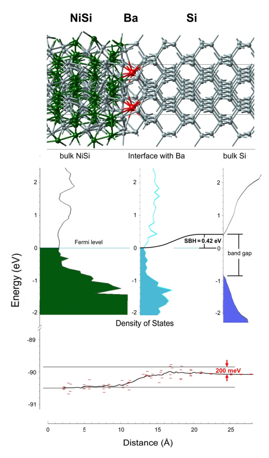
Figure 19.2.2 Atomic structure of the interface NiSi/Ba/Si(top), LDOS (middle), and layer-decomposed Si-2p energy states (bottom). Note the reduction of the Schottky barrier by 200 meV compared with the undoped system.
19.3. Electronic Structure of NiSi/Si
The computed alignment of electronic states for the NiSi/Si interface is displayed in Figure 19.2.1 in terms of the layer-decomposed density of states (LDOS). Inside the NiSi region the LDOS has the form of that of bulk NiSi and, correspondingly, the LDOS inside the Si region is that of pure Si bulk. The calculations reveal that the Si bands align such that the Fermi level of the metal ends up near the middle of the Si band gap. The effective potential rises smoothly so that the Schottky barrier height \(\Phi\)bn is the difference between the bottom of the conduction band and the Fermi level. The rise of the potential is monitored by the computed Si-2p energy levels shown for each layer of the NiSi/Si interface at the bottom of Figure 19.1.1. The computed value of the SBH, \(\Phi\)bn, is 0.62 eV, which is in excellent agreement with the experimental value of 0.65 eV reported in [2]. It should be noted that the geometric structure of an interface such as NiSi/Si as well as the equilibrium position of dopant atoms such as Ba and S can be computed using standard DFT-GGA calculations. This level of theory also describes correctly the charge density of the system and consequently the resulting interface dipole. Obtaining the correct band gap for the semiconductor requires a step beyond DFT. This can be accomplished by applying a scissors operator, i.e. shfting the conducation band up, or by performing hybrid functional calculations. Anyhow, the core level shifts across the interface as shown in the figures of this application note as well as the dopant-induced changes of the Schottky barrier are properly described at the DFT-GGA level of theory since those are ground state properties of the system. Hence, it is actually not necessary to perform computationally demanding hybrid functional calculations to predict dopant-induced shifts of the Schottky barrier.
19.4. Electronic Structure of NiSi/Ba/Si
With MedeA one can predict the effect of dopant atoms on the SBH, as shown here for the case of Ba at the NiSi/Si interface. In general the effect of the dopant atoms is most conveniently monitored by core level shifts such as the Si-2p energy levels inside the Si region relative to the reference energy levels inside NiSi. As shown in Figure 19.2.1 and Figure 19.2.2 the calculations reveal that the electronic energy levels inside Si are shifted by 200 meV to lower energies relative to the reference levels inside NiSi. As a consequence, the valence band minimum moves closer to the Fermi level and the SBH \(\Phi\)bn, is reduced from 0.62 eV to 0.42 eV.
19.5. Location of dopants at the NiSi/Si interface
Using the atomistic simulation techniques of the MedeA Environment the energetically most stable positions of any dopant atom or impurity can be determined. In case of NiSi/Ba/Si it was assumed that the dopant atom is located near the interface, but a priori it is unknown where dopant or impurity atoms are located. For instance, calculations on NiSi/Si interfaces with sulfur impurities show that the S atoms energetically prefer the region near the interface, but also could remain inside the silicide. They are energetically less stable inside bulk Si. If S is implanted into Si prior to the formation of nickel silicide, it is likely that during the silicidation process S atoms accumulate at the NiSi/Si interface, but also get incorporated in the NiSi phase. In fact, the role of dopant atoms such as sulfur in tuning the SBH in NiSi/Si systems is an area of active research [3].
19.6. Significance
Atomistic simulations with MedeA have a high predictive power in understanding and controlling the contact resistance in electronic devices. Electronic structure calculations, which can be routinely performed using MedeA VASP, are increasingly employed industrially (see, for example, the patent application of Toshiba [4]). The need for an atomistic level understanding is amplified by the increasing materials diversity and the decreasing dimensions of modern electronic devices.
The methodology [5] implemented in MedeA is generally applicable in case of a large number of different materials, interfaces, and dopants, thus providing a unique tool for the interpretation of existing experimental data and, perhaps more importantly, for focusing new experiments on the most promising candidates.
The calculations described in this application note set the stage for simulating more complex systems including, e.g. n- and p-doping of the semiconductor, thus capturing effects such as band bending.
MedeA Modules Used in this Application
- MedeA Environment
- MedeA Interface Builder
- MedeA VASP
| [1] | MedeA and Materials Design are registered trademarks of Materials Design, Inc. |
| [2] | (1, 2) Q. T. Zhao, U. Breuer, E. Rije, St. Lenk, and S. Mantl, “Tuning of NiSi/Si Schotty barrier heights by sulfur segregation during Ni silicidation”, Appl. Phys. Lett. 86, 062108 (2005) (DOI) |
| [3] | J. Chan, N. Y. Martinez, J. J. D. Fitzgerald, A. V. Walker, R. A. Chapman, D. Riley, A. Jain, C. L. Hinkle, and E. M. Vogel, “Extraction of correct Schottky barrier height of sulfur implanted NiSi/n-Si junctions: Junction doping rather than barrier height lowering”, Appl. Phys. Lett. 99, 012114 (2011) (DOI) |
| [4] | US Patent Application No. US 2009/0134388 A1, May 2009 |
| [5] | J. Hafner, “Ab-initio simulations of materials using VASP: Density-functional theory and beyond”, J. Comput. Chem. 29, 2044 (2008) and references therein (DOI) |
| download: | pdf |
|---|